How Microchips are Made

Used in almost everything humans rely on in their day-to-day lives, to make a microchip, you begin with raw polysilicon heated to 1,420 degrees celsius inside a vacuum-sealed furnace purged of oxygen. The molten silicon is then spun in a centrifuge, before a pencil-thin silicon seed crystal is lowered into the soup while spinning in the opposite direction.
The Process Begins
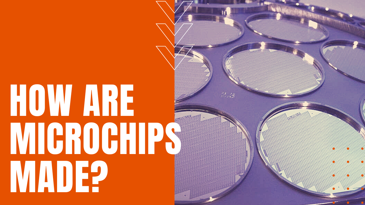
As the molten polysilicon is allowed to cool, the seed crystal is withdrawn at approximately 1/16th of an inch per minute, resulting in a single and quite massive silicon crystal weighing upwards of 440 pounds, with a diameter of nearly eight inches. The crystal is then carefully reoriented and sliced into razor thin wafers of pure silicon 2/3 of a mm thick. The wafers are then placed in a lapping polisher, followed by a secondary chemical buffing that results in a product that lacks any appreciable surface roughness.
Fabrication Facilities
The wafers are then transported to a fabrication facility, where they undergo some 1,500 processing steps from start to finish, all within a Class One clean room environment approximately 1,000 times cleaner than a hospital operating room. Since a single particle of dust can prove catastrophic to the health of a microchip, throughout the processing cycle, chips are further isolated from dust-producing workers through the use of front opening unified pods or “FOUPS,” which ferry wafers from machine to machine through their processing cycle.
Incredible Density
While the first microchip had one transistor and three resistors on its semiconductor base, today’s chips pack billions of transistors onto wafers as small as 4 nanometers, including Apple’s 2022 release of their M1 Ultra chip, which boasts a staggering 114 billion transistors on a 5 nanometer base. To achieve such incredible transistor density on such tiny platforms requires a process known as photo lithography, where chips are coated with photo sensitive chemicals, which harden when exposed to UV light.
Microscopic Technology
Transferred into a sealed darkroom, light is shown through an image of the chip’s intended circuit design, beamed through a miniaturizing lens, which then etches the design onto the coated wafer. The FOUPS repeat this photo etching process as many as forty times under a variety of different layering techniques, creating silicon wafers that sport as many as 1,000 microchips per finished wafer, with over 4,000 billion circuit elements, making the modern microchip a vital mainstay of 21st century life.
